 | –≠–ª–µ–∫—Ç—Ä–æ–Ω–Ω—ã–π –∫–æ–º–ø–æ–Ω–µ–Ω—Ç: MT4C4M4E8 | –°–∫–∞—á–∞—Ç—å:  PDF PDF  ZIP ZIP |
4 Meg x 4 EDO DRAM
Micron Technology, Inc., reserves the right to change products or specifications without notice.
D47.pm5 ≠ Rev. 3/97
©
1997, Micron Technology, Inc.
1
4 MEG x 4
EDO DRAM
TECHNOLOGY, INC.
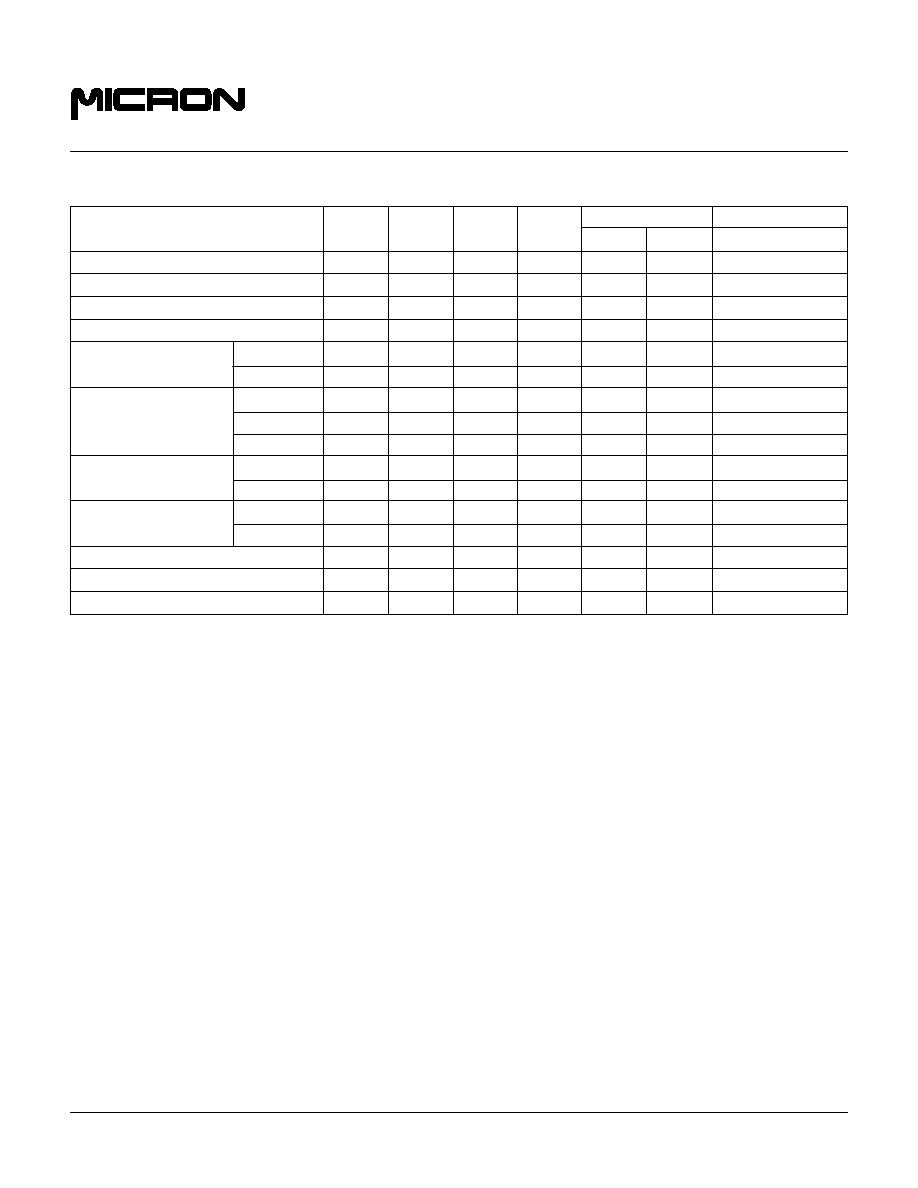
4 MEG x 4 EDO DRAM PART NUMBERS
PART NUMBER
Vcc
REFRESH
PACKAGE
REFRESH
MT4LC4M4E8DJ
3.3V
2K
SOJ
Standard
MT4LC4M4E8DJS
3.3V
2K
SOJ
Self
MT4LC4M4E8TG
3.3V
2K
TSOP
Standard
MT4LC4M4E8TGS
3.3V
2K
TSOP
Self
MT4LC4M4E9DJ
3.3V
4K
SOJ
Standard
MT4LC4M4E9DJS
3.3V
4K
SOJ
Self
MT4LC4M4E9TG
3.3V
4K
TSOP
Standard
MT4LC4M4E9TGS
3.3V
4K
TSOP
Self
MT4C4M4E8DJ
5V
2K
SOJ
Standard
MT4C4M4E8DJS
5V
2K
SOJ
Self
MT4C4M4E8TG
5V
2K
TSOP
Standard
MT4C4M4E8TGS
5V
2K
TSOP
Self
MT4C4M4E9DJ
5V
4K
SOJ
Standard
MT4C4M4E9DJS
5V
4K
SOJ
Self
MT4C4M4E9TG
5V
4K
TSOP
Standard
MT4C4M4E9TGS
5V
4K
TSOP
Self
MT4LC4M4E8, MT4C4M4E8
MT4LC4M4E9, MT4C4M4E9
DRAM
FEATURES
∑ Industry-standard x4 pinout, timing, functions and
packages
∑ State-of-the-art, high-performance, low-power CMOS
silicon-gate process
∑ Single power supply (+3.3V
±
0.3V or +5V
±
10%)
∑ All inputs, outputs and clocks are TTL-compatible
∑ Refresh modes: RAS#-ONLY, HIDDEN and CAS#-
BEFORE-RAS# (CBR)
∑ Optional Self Refresh (S) for low-power data retention
∑ 11 row, 11 column addresses (2K refresh) or
12 row, 10 column addresses (4K refresh)
∑ Extended Data-Out (EDO) PAGE MODE access cycle
∑ 5V-tolerant inputs and I/Os on 3.3V devices
OPTIONS
MARKING
∑ Voltages
3.3V
LC
5V
C
∑ Refresh Addressing
2,048 (i.e. 2K) Rows
E8
4,096 (i.e. 4K) Rows
E9
∑ Packages
Plastic SOJ (300 mil)
DJ
Plastic TSOP (300 mil)
TG
∑ Timing
50ns access
-5
60ns access
-6
∑ Refresh Rates
Standard Refresh
None
Self Refresh (128ms period)
S
∑ Part Number Example: MT4LC4M4E8DJ-6
Note:
The 4 Meg x 4 EDO DRAM base number differentiates the offerings in
two places - MT4LC4M4E8. The third field distinguishes the low voltage
offering: LC designates V
CC
= 3.3V and C designates V
CC
= 5V. The fifth field
distinguishes various options: E8 designates a 2K refresh and E9 designates a
4K refresh for EDO DRAMs.
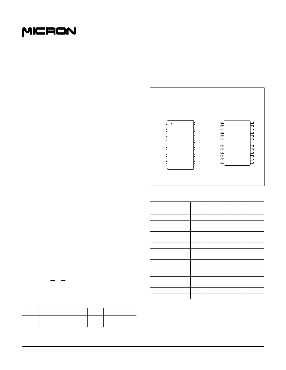
PIN ASSIGNMENT (Top View)
24/26-Pin SOJ
(DA-2)
V
CC
DQ1
DQ2
WE#
RAS#
*NC/A11
A10
A0
A1
A2
A3
V
CC
1
2
3
4
5
6
8
9
10
11
12
13
26
25
24
23
22
21
19
18
17
16
15
14
V
SS
DQ4
DQ3
CAS#
OE#
A9
A8
A7
A6
A5
A4
V
SS
V
CC
DQ1
DQ2
WE#
RAS#
*NC/A11
A10
A0
A1
A2
A3
V
CC
1
2
3
4
5
6
8
9
10
11
12
13
26
25
24
23
22
21
19
18
17
16
15
14
V
SS
DQ4
DQ3
CAS#
OE#
A9
A8
A7
A6
A5
A4
V
SS
24/26-Pin TSOP
(DB-2)
* NC on 2K refresh and A11 on 4K refresh options.
GENERAL DESCRIPTION
The 4 Meg x 4 DRAM is a randomly accessed, solid-state
memory containing 16,777,216 bits organized in a x4 con-
figuration. RAS# is used to latch the row address (first 11
bits for 2K and first 12 bits for 4K). Once the page has been
opened by RAS#, CAS# is used to latch the column address
KEY TIMING PARAMETERS
SPEED
t
RC
t
RAC
t
PC
t
AA
t
CAC
t
CAS
-5
84ns
50ns
20ns
25ns
13ns
8ns
-6
104ns
60ns
25ns
30ns
15ns
10ns
Note:
The "#" symbol indicates signal is active LOW.
4 Meg x 4 EDO DRAM
Micron Technology, Inc., reserves the right to change products or specifications without notice.
D47.pm5 ≠ Rev. 3/97
©
1997, Micron Technology, Inc.
2
4 MEG x 4
EDO DRAM
TECHNOLOGY, INC.
GENERAL DESCRIPTION (continued)
(the latter 11 bits for 2K and the latter 10 bits for 4K, address
pins A10 and A11 are "don't care"). READ and WRITE
cycles are selected with the WE# input.
A logic HIGH on WE# dictates READ mode, while a logic
LOW on WE# dictates WRITE mode. During a WRITE
cycle, data-in (D) is latched by the falling edge of WE# or
CAS#, whichever occurs last. An EARLY WRITE occurs
when WE# is taken LOW prior to CAS# falling. A LATE
WRITE or READ-MODIFY-WRITE occurs when WE# falls
after CAS# is taken LOW. During EARLY WRITE cycles,
the data outputs (Q) will remain High-Z regardless of the
state of OE#. During LATE WRITE or READ-MODIFY-
WRITE cycles, OE# must be taken HIGH to disable the data
outputs prior to applying input data. If a LATE WRITE or
READ-MODIFY-WRITE is attempted while keeping OE#
LOW, no write will occur, and the data outputs will drive
read data from the accessed location.
The four data inputs and the four data outputs are routed
through four pins using common I/O, and pin direction is
controlled by WE# and OE#.
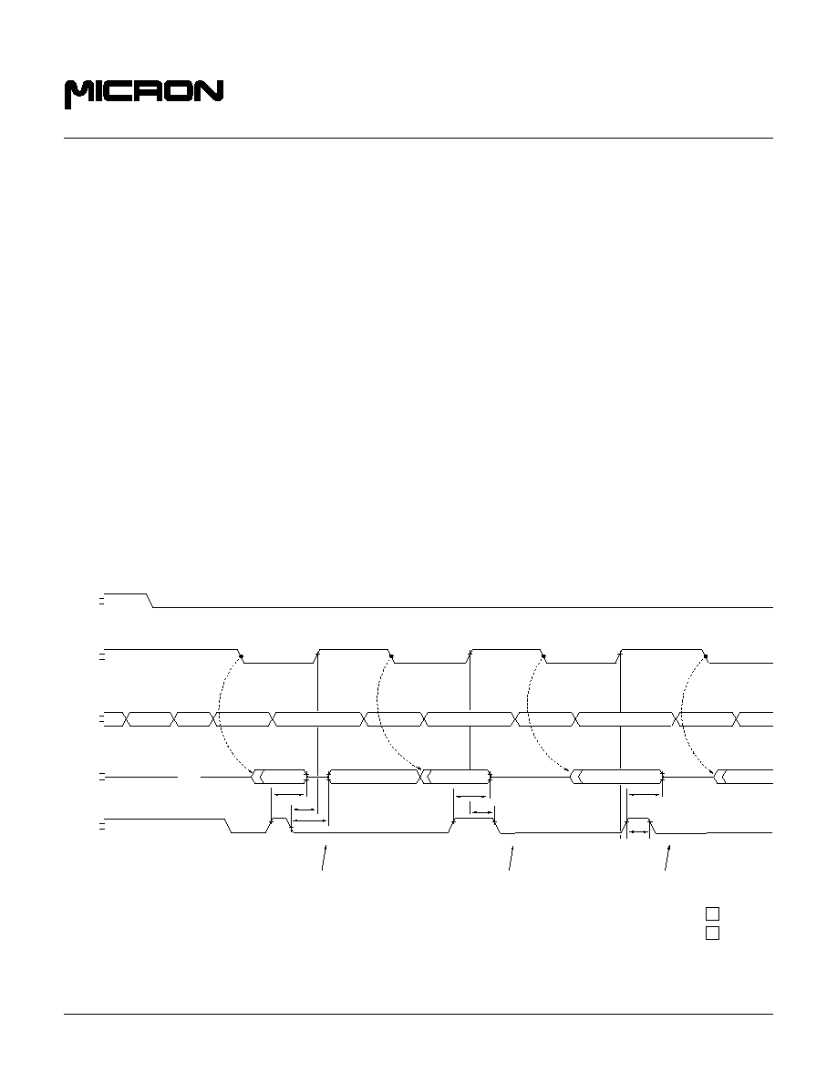
PAGE ACCESS
PAGE operations allow faster data operations (READ,
WRITE or READ-MODIFY-WRITE) within a row address-
defined page boundary. The PAGE cycle is always initiated
Figure 1
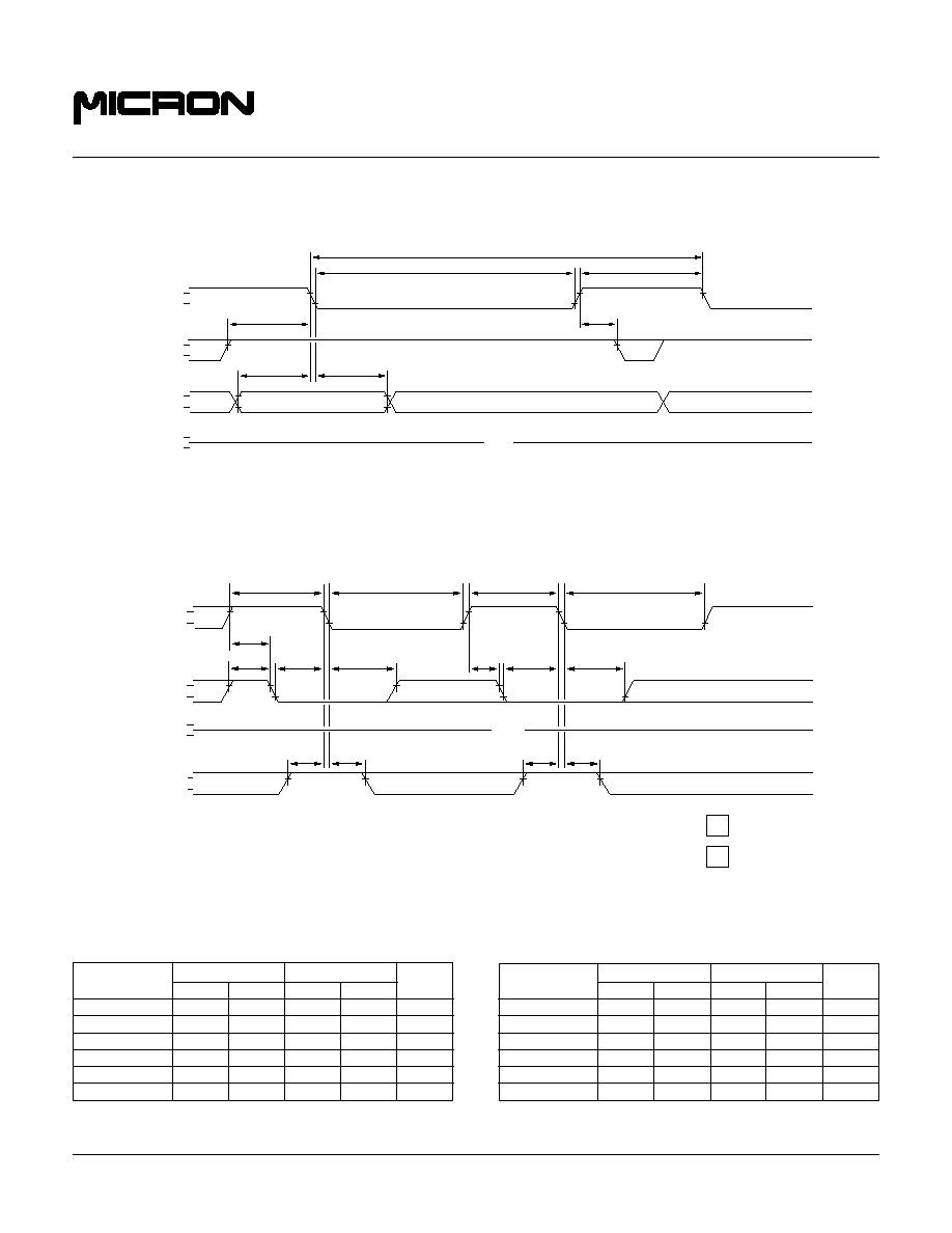
OE# CONTROL OF DQs
with a row address strobed-in by RAS#, followed by a
column address strobed-in by CAS#. CAS# may be
toggled-in by holding RAS# LOW and strobing-in different
column addresses, thus executing faster memory cycles.
Returning RAS# HIGH terminates the PAGE MODE of
operation, i.e., closes the page.
EDO PAGE MODE
The 4 Meg x 4 EDO DRAM provides EDO PAGE MODE,
which is an accelerated FAST PAGE MODE cycle. The
primary advantage of EDO is the availability of data-out
even after CAS# returns HIGH. EDO allows CAS# precharge
time (
t
CP) to occur without the output data going invalid.
This elimination of CAS# output control allows pipeline
READs.
FAST PAGE MODE DRAMs have traditionally turned
the output buffers off (High-Z) with the rising edge of
CAS#. EDO PAGE MODE DRAMs operate like FAST
PAGE MODE DRAMs, except data will remain valid or
become valid after CAS# goes HIGH during READs, pro-
vided RAS# and OE# are held LOW. If OE# is pulsed while
RAS# and CAS# are LOW, data will toggle from valid data
to High-Z and back to the same valid data. If OE# is toggled
or pulsed after CAS# goes HIGH while RAS# remains
LOW, data will transition to and remain High-Z (refer to
,,
,,,
V
V
IH
IL
CAS#
V
V
IH
IL
RAS#
V
V
IH
IL
ADDR
,,
ROW
,,
,
COLUMN (A)
,,
,,,
,,
COLUMN (B)
,
,,,,
,,
DON'T CARE
UNDEFINED
,
,
,,
,,
V
V
IH
IL
OE#
V
V
IOH
IOL
OPEN
DQ
tOD
VALID DATA (B)
VALID DATA (A)
,
COLUMN (C)
,,,
,,,
VALID DATA (A)
tOE
,,
VALID DATA (C)
,
COLUMN (D)
,,,
,,
,
VALID DATA (D)
tOD
tOEHC
tOD
tOEP
tOES
The DQs go back to
Low-Z if
t
OES is met.
The DQs remain High-Z
until the next CAS# cycle
if
t
OEHC is met.
The DQs remain High-Z
until the next CAS# cycle
if
t
OEP is met.
4 Meg x 4 EDO DRAM
Micron Technology, Inc., reserves the right to change products or specifications without notice.
D47.pm5 ≠ Rev. 3/97
©
1997, Micron Technology, Inc.
3
4 MEG x 4
EDO DRAM
TECHNOLOGY, INC.
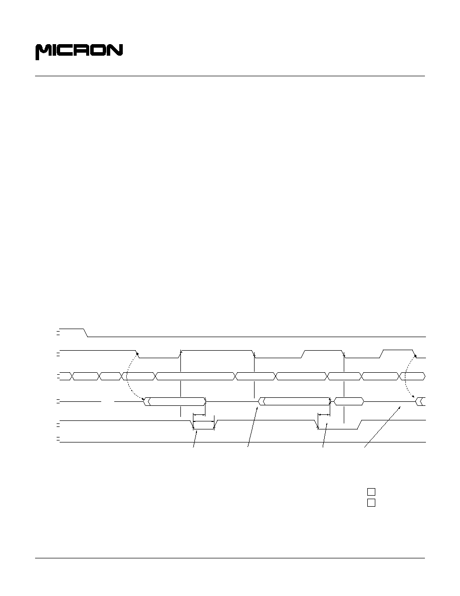
Figure 1). WE# can also perform the function of disabling
the output devices under certain conditions, as shown in
Figure 2.
During an application, if the DQ outputs are wire OR'd,
OE# must be used to disable idle banks of DRAMs. Alter-
natively, pulsing WE# to the idle banks during CAS# high
time will also High-Z the outputs. Independent of OE#
control, the outputs will disable after
t
OFF, which is refer-
enced from the rising edge of RAS# or CAS#, whichever
occurs last.
REFRESH
Preserve correct memory cell data by maintaining power
and executing any RAS# cycle (READ, WRITE) or RAS#
refresh cycle (RAS#-ONLY, CBR or HIDDEN) so that all
combinations of RAS# addresses (2,048 for 2K and 4,096 for
4K) are executed within
t
REF (MAX), regardless of se-
quence. The CBR and Self Refresh cycles will invoke the
internal refresh counter for automatic RAS# addressing.
An optional Self Refresh mode is also available on the S
version. The "S" option allows the user the choice of a fully
static, low-power data retention mode or a dynamic refresh
mode at the extended refresh period of 128ms. The optional
Self Refresh feature is initiated by performing a CBR Re-
fresh cycle and holding RAS# LOW for the specified
t
RASS.
Additionally, the "S" option allows for an extended refresh
period of 128ms, or 31.25
µ
s per row for a 4K refresh and
62.5
µ
s per row for a 2K refresh if using distributed CBR
Refresh. This refresh rate can be applied during normal
operation, as well as during a standby or BATTERY BACKUP
mode.
The Self Refresh mode is terminated by driving RAS#
HIGH for a minimum time of
t
RPS. This delay allows for the
completion of any internal refresh cycles that may be in
process at the time of the RAS# LOW-to-HIGH transition.
If the DRAM controller uses a distributed refresh se-
quence, a burst refresh is not required upon exiting
Self Refresh. However, if the DRAM controller utilizes a
RAS#- ONLY or burst refresh sequence, all rows must be
refreshed within the average internal refresh rate, prior to
the resumption of normal operation.
STANDBY
Returning RAS# and CAS# HIGH terminates a memory
cycle and decreases chip current to a reduced standby level.
The chip is preconditioned for the next cycle during the
RAS# HIGH time.
Figure 2
WE# CONTROL OF DQs
,,
,,
V
V
IH
IL
CAS#
V
V
IH
IL
RAS#
V
V
IH
IL
ADDR
,,
ROW
,,
,
COLUMN (A)
,,
,,,
,
DON'T CARE
UNDEFINED
,
,,
,,
,,
V
V
IH
IL
WE#
V
V
IOH
IOL
OPEN
DQ
,
,
,
,,,
,
,,
,,
,,
,,
tWPZ
The DQs go to High-Z if WE# falls and, if
t
WPZ is met,
will remain High-Z until CAS# goes LOW with
WE# HIGH (i.e., until a READ cycle is initiated).
V
V
IH
IL
OE#
,
,
VALID DATA (B)
t
WHZ
WE# may be used to disable the DQs to prepare
for input data in an EARLY WRITE cycle. The DQs
will remain High-Z until CAS# goes LOW with
WE# HIGH (i.e., until a READ cycle is initiated).
t
WHZ
COLUMN (D)
,,
,,,
,,,
VALID DATA (A)
COLUMN (B)
COLUMN (C)
INPUT DATA (C)
4 Meg x 4 EDO DRAM
Micron Technology, Inc., reserves the right to change products or specifications without notice.
D47.pm5 ≠ Rev. 3/97
©
1997, Micron Technology, Inc.
4
4 MEG x 4
EDO DRAM
TECHNOLOGY, INC.
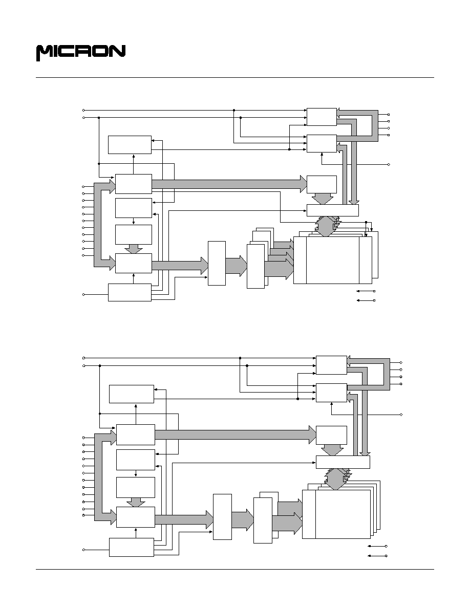
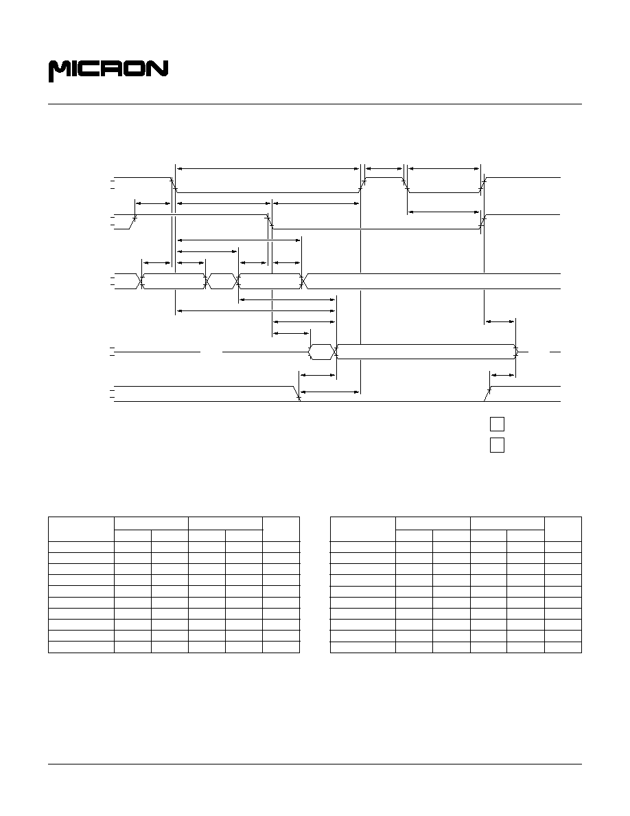
FUNCTIONAL BLOCK DIAGRAM - 2K REFRESH
2048
2048
A0
A1
A2
A3
A4
A5
A6
A7
A8
A9
A10
RAS#
11
11
11
NO. 2 CLOCK
GENERATOR
REFRESH
CONTROLLER
NO. 1 CLOCK
GENERATOR
V
DD
V
SS
11
WE#
CAS#
10
COLUMN
ADDRESS
BUFFER(11)
ROW
ADDRESS
BUFFERS (11)
2048
ROW
DECODER
2048
1024
COLUMN
DECODER
OE#
DQ1
DQ2
DQ3
DQ4
4
4
4
4
REFRESH
COUNTER
1
ROW TRANSFER
(1 OF 2)
ROW TRANSFER
(1 OF 2)
1024
4096 x 1024 x 4
MEMORY
ARRAY
SENSE AMPLIFIERS
I/O GATING
DATA-OUT
BUFFER
DATA-IN
BUFFER
COMPLEMENT
SELECT
2048
ROW SELECT
(2 of 4096)
FUNCTIONAL BLOCK DIAGRAM - 4K REFRESH
4096
A0
A1
A2
A3
A4
A5
A6
A7
A8
A9
A10
A11
RAS#
12
12
10
NO. 2 CLOCK
GENERATOR
REFRESH
CONTROLLER
NO. 1 CLOCK
GENERATOR
V
DD
V
SS
12
WE#
CAS#
10
COLUMN
ADDRESS
BUFFER(10)
ROW
ADDRESS
BUFFERS (12)
ROW
DECODER
4096
1024
COLUMN
DECODER
OE#
DQ1
DQ2
DQ3
DQ4
4
4
4
4
REFRESH
COUNTER
1024
4096 x 1024 x 4
MEMORY
ARRAY
SENSE AMPLIFIERS
I/O GATING
DATA-OUT
BUFFER
DATA-IN
BUFFER
COMPLEMENT
SELECT
4096
ROW SELECT
(1 of 4096)
4 Meg x 4 EDO DRAM
Micron Technology, Inc., reserves the right to change products or specifications without notice.
D47.pm5 ≠ Rev. 3/97
©
1997, Micron Technology, Inc.
5
4 MEG x 4
EDO DRAM
TECHNOLOGY, INC.
TRUTH TABLE
ADDRESSES
DATA-IN/OUT
FUNCTION
RAS#
CAS#
WE#
OE#
t
R
t
C
DQ1-DQ4
Standby
H
H
X
X
X
X
X
High-Z
READ
L
L
H
L
ROW
COL
Data-Out
EARLY WRITE
L
L
L
X
ROW
COL
Data-In
READ WRITE
L
L
H
L
L
H
ROW
COL
Data-Out, Data-In
EDO-PAGE-MODE
1st Cycle
L
H
L
H
L
ROW
COL
Data-Out
READ
2nd Cycle
L
H
L
H
L
n/a
COL
Data-Out
EDO-PAGE-MODE
1st Cycle
L
H
L
L
X
ROW
COL
Data-In
EARLY WRITE
2nd Cycle
L
H
L
L
X
n/a
COL
Data-In
Any Cycle
L
L
H
H
L
n/a
n/a
Data-Out
EDO-PAGE-MODE
1st Cycle
L
H
L
H
L
L
H
ROW
COL
Data-Out, Data-In
READ-WRITE
2nd Cycle
L
H
L
H
L
L
H
n/a
COL
Data-Out, Data-In
HIDDEN
READ
L
H
L
L
H
L
ROW
COL
Data-Out
REFRESH
WRITE
L
H
L
L
L
X
ROW
COL
Data-In
RAS#-ONLY REFRESH
L
H
X
X
ROW
n/a
High-Z
CBR REFRESH
H
L
L
H
X
X
X
High-Z
SELF REFRESH
H
L
L
H
X
X
X
High-Z
4 Meg x 4 EDO DRAM
Micron Technology, Inc., reserves the right to change products or specifications without notice.
D47.pm5 ≠ Rev. 3/97
©
1997, Micron Technology, Inc.
6
4 MEG x 4
EDO DRAM
TECHNOLOGY, INC.
ABSOLUTE MAXIMUM RATINGS*
Voltage on V
CC
Pin Relative to V
SS
:
3.3V ................................................................ -1V to +4.6V
5V ...................................................................... -1V to +7V
Voltage on NC, Inputs or I/O Pins Relative to V
SS
:
3.3V ................................................................ -1V to +5.5V
5V ...................................................................... -1V to +7V
Operating Temperature, T
A
(ambient) .......... 0
∞
C to +70
∞
C
Storage Temperature (plastic) .................... -55
∞
C to +150
∞
C
Power Dissipation ............................................................. 1W
Short Circuit Output Current ..................................... 50mA
*Stresses greater than those listed under "Absolute Maxi-
mum Ratings" may cause permanent damage to the device.
This is a stress rating only and functional operation of the
device at these or any other conditions above those indi-
cated in the operational sections of this specification is not
implied. Exposure to absolute maximum rating conditions
for extended periods may affect reliability.
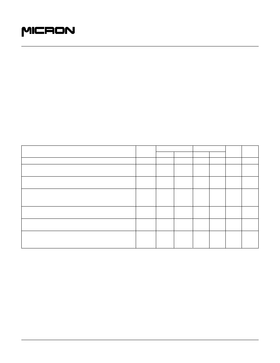
DC ELECTRICAL CHARACTERISTICS AND OPERATING CONDITIONS
(Notes: 1)
3.3V
5V
PARAMETER/CONDITION
SYMBOL
MIN
MAX
MIN
MAX
UNITS
NOTES
Supply Voltage
V
CC
3.0
3.6
4.5
5.5
V
Input High Voltage:
Valid Logic 1; all inputs, I/Os and any NC
V
IH
2.0
5.5
2.4
V
CC
+1
V
Input Low Voltage:
Valid Logic 0; all inputs, I/Os and any NC
V
IL
-1.0
0.8
-0.5 0.8
V
Input Leakage Current:
Any input at V
IN
(0V
V
IN
V
IH
[MAX]);
I
I
-2
2
-2
2
µ
A
4
all other pins not under test = 0V
Output High Voltage:
I
OUT
= -2mA (3.3V), -5mA (5V)
V
OH
2.4
-
2.4
-
V
Output Low Voltage:
I
OUT
= 2mA (3.3V), 4.2mA (5V)
V
OL
-
0.4
-
0.4
V
Output Leakage Current:
Any output at V
OUT
(0V
V
OUT
5.5V);
I
OZ
-5
5
-5
5
µ
A
DQ is disabled and in High-Z state
4 Meg x 4 EDO DRAM
Micron Technology, Inc., reserves the right to change products or specifications without notice.
D47.pm5 ≠ Rev. 3/97
©
1997, Micron Technology, Inc.
7
4 MEG x 4
EDO DRAM
TECHNOLOGY, INC.
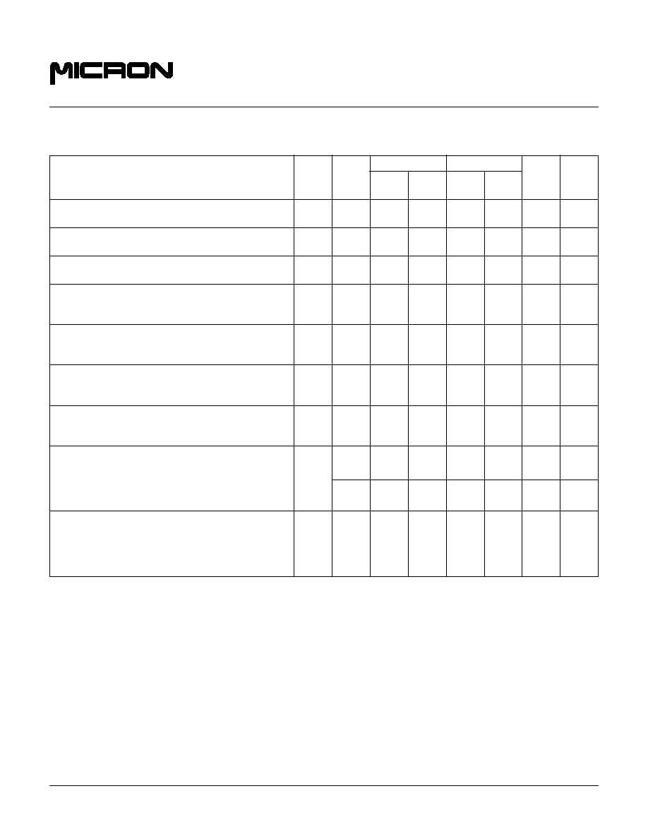
Icc OPERATING CONDITIONS AND MAXIMUM LIMITS
(Notes: 1, 2, 3)
3.3V
5V
2K
4K
2K
4K
PARAMETER/CONDITION
SYM
SPEED Refresh Refresh Refresh Refresh
UNITS
NOTES
STANDBY CURRENT: TTL
I
CC
1
ALL
1
1
1
1
mA
(RAS# = CAS# = V
IH
)
STANDBY CURRENT: CMOS (non-S version only)
I
CC
2
ALL
500
500
500
500
µ
A
(RAS# = CAS# = other inputs = V
CC
-0.2V)
STANDBY CURRENT: CMOS (S version only)
I
CC
2
ALL
150
150
150
150
µ
A
(RAS# = CAS# = other inputs = V
CC
-0.2V)
OPERATING CURRENT: Random READ/WRITE
-5
110
90
140
120
mA
5, 6
Average power supply current
I
CC
3
-6
100
80
130
110
(RAS#, CAS#, address cycling:
t
RC =
t
RC [MIN])
OPERATING CURRENT: EDO PAGE MODE
-5
110
100
110
100
mA
5, 6
Average power supply current (RAS# = V
IL
,
I
CC
4
-6
100
90
100
90
CAS#, address cycling:
t
PC =
t
PC [MIN])
REFRESH CURRENT: RAS#-ONLY
-5
110
90
140
120
mA
5, 6
Average power supply current
I
CC
5
-6
100
80
130
110
(RAS# cycling, CAS# = V
IH
:
t
RC =
t
RC [MIN])
REFRESH CURRENT: CBR
-5
110
90
140
120
mA
5, 7
Average power supply current
I
CC
6
-6
100
80
130
110
(RAS#, CAS#, address cycling:
t
RC =
t
RC [MIN])
REFRESH CURRENT: Extended (S version only)
Average power supply current: CAS# = 0.2V or
ALL
300
300
300
300
µ
A
5, 7
CBR cycling; RAS# =
t
RAS (MIN); WE# =
I
CC
7
V
CC
-0.2V; A0-A11,OE# and D
IN
= V
CC
-0.2V or
t
RC
62.5
31.25
62.5
31.25
µ
s
25
0.2V (D
IN
may be left open)
REFRESH CURRENT: Self (S version only)
Average power supply current: CBR with
RAS#
t
RASS (MIN) and CAS# held LOW; WE# =
I
CC
8
ALL
300
300
300
300
µ
A
5, 7
V
CC
-0.2V; A0-A11, OE# and D
IN
= V
CC
-0.2V
or 0.2V (D
IN
may be left open)

4 Meg x 4 EDO DRAM
Micron Technology, Inc., reserves the right to change products or specifications without notice.
D47.pm5 ≠ Rev. 3/97
©
1997, Micron Technology, Inc.
8
4 MEG x 4
EDO DRAM
TECHNOLOGY, INC.
AC ELECTRICAL CHARACTERISTICS
(Notes: 2, 3, 9, 10, 11, 12, 17) (V
CC
[MIN]
V
CC
V
CC
[MAX])
AC CHARACTERISTICS
-5
-6
PARAMETER
SYMBOL
MIN
MAX
MIN
MAX
UNITS
NOTES
Access time from column address
t
AA
25
30
ns
Column address setup to CAS# precharge
t
ACH
12
15
ns
Column address hold time (referenced to RAS#)
t
AR
38
45
ns
Column address setup time
t
ASC
0
0
ns
Row address setup time
t
ASR
0
0
ns
Column address to WE# delay time
t
AWD
42
49
ns
13
Access time from CAS#
t
CAC
13
15
ns
14
Column address hold time
t
CAH
8
10
ns
CAS# pulse width
t
CAS
8
10,000
10
10,000
ns
CAS# LOW to "don't care" during Self Refresh
t
CHD
15
15
ns
CAS# hold time (CBR Refresh)
t
CHR
8
10
ns
7
CAS# to output in Low-Z
t
CLZ
0
0
ns
Data output hold after next CAS# LOW
t
COH
3
3
ns
CAS# precharge time
t
CP
8
10
ns
15
Access time from CAS# precharge
t
CPA
28
35
ns
CAS# to RAS# precharge time
t
CRP
5
5
ns
CAS# hold time
t
CSH
38
45
ns
CAS# setup time (CBR Refresh)
t
CSR
5
5
ns
CAS# to WE# delay time
t
CWD
28
35
ns
13
Write command to CAS# lead time
t
CWL
8
10
ns
Data-in hold time
t
DH
8
10
ns
16
Data-in setup time
t
DS
0
0
ns
16
Output disable
t
OD
0
12
0
15
ns
Output Enable
t
OE
12
15
ns
17
OE# hold time from WE# during
t
OEH
8
10
ns
18
READ-MODIFY-WRITE cycle
OE# HIGH hold from CAS# HIGH
t
OEHC
5
10
ns
18
OE# HIGH pulse width
t
OEP
5
5
ns
OE# LOW to CAS# HIGH setup time
t
OES
4
5
ns
Output buffer turn-off delay
t
OFF
0
12
0
15
ns
20
CAPACITANCE
PARAMETER
SYMBOL
MAX
UNITS
NOTES
Input Capacitance: Address pins
C
I
1
5
pF
8
Input Capacitance: RAS#, CAS#, WE#, OE#
C
I
2
7
pF
8
Input/Output Capacitance: DQ
C
IO
7
pF
8
4 Meg x 4 EDO DRAM
Micron Technology, Inc., reserves the right to change products or specifications without notice.
D47.pm5 ≠ Rev. 3/97
©
1997, Micron Technology, Inc.
9
4 MEG x 4
EDO DRAM
TECHNOLOGY, INC.
AC ELECTRICAL CHARACTERISTICS
(Notes: 2, 3, 9, 10, 11, 12, 17) (V
CC
[MIN]
V
CC
V
CC
[MAX])
AC CHARACTERISTICS
-5
-6
PARAMETER
SYMBOL
MIN
MAX
MIN
MAX
UNITS
NOTES
OE# setup prior to RAS# during
t
ORD
0
0
ns
HIDDEN REFRESH cycle
EDO-PAGE-MODE READ or WRITE cycle time
t
PC
20
25
ns
EDO-PAGE-MODE READ-WRITE cycle time
t
PRWC
47
56
ns
Access time from RAS#
t
RAC
50
60
ns
19
RAS# to column address delay time
t
RAD
9
12
ns
21
Row address hold time
t
RAH
9
10
ns
RAS# pulse width
t
RAS
50
10,000
60
10,000
ns
RAS# pulse width (EDO PAGE MODE)
t
RASP
50
125,000
60
125,000
ns
RAS# pulse width during Self Refresh
t
RASS
100
100
µ
s
Random READ or WRITE cycle time
t
RC
84
104
ns
RAS# to CAS# delay time
t
RCD
11
14
ns
22
Read command hold time (referenced to CAS#)
t
RCH
0
0
ns
23
Read command setup time
t
RCS
0
0
ns
Refresh period (2,048 cycles)
t
REF
32
32
ms
Refresh period (4,096 cycles)
t
REF
64
64
ms
Refresh period S version
t
REF
128
128
ms
RAS# precharge time
t
RP
30
40
ns
RAS# to CAS# precharge time
t
RPC
5
5
ns
RAS# precharge time exiting Self Refresh
t
RPS
90
105
ns
Read command hold time (referenced to RAS#)
t
RRH
0
0
ns
23
RAS# hold time
t
RSH
13
15
ns
READ WRITE cycle time
t
RWC
116
140
ns
RAS# to WE# delay time
t
RWD
67
79
ns
13
Write command to RAS# lead time
t
RWL
13
15
ns
Transition time (rise or fall)
t
T
2
50
2
50
ns
Write command hold time
t
WCH
8
10
ns
Write command hold time (referenced to RAS#)
t
WCR
38
45
ns
WE# command setup time
t
WCS
0
0
ns
13
Output disable delay from WE#
t
WHZ
0
12
0
15
ns
Write command pulse width
t
WP
5
5
ns
WE# pulse to disable at CAS# HIGH
t
WPZ
10
10
ns
WE# hold time (CBR Refresh)
t
WRH
8
10
ns
WE# setup time (CBR Refresh)
t
WRP
8
10
ns

4 Meg x 4 EDO DRAM
Micron Technology, Inc., reserves the right to change products or specifications without notice.
D47.pm5 ≠ Rev. 3/97
©
1997, Micron Technology, Inc.
10
4 MEG x 4
EDO DRAM
TECHNOLOGY, INC.
NOTES
1. All voltages referenced to V
SS
.
2. The minimum specifications are used only to indicate
cycle time at which proper operation over the full
temperature range (0∞C
T
A
70∞C) is ensured.
3. An initial pause of 100
µ
s is required after power-up,
followed by eight RAS# refresh cycles (RAS#-ONLY
or CBR with WE# HIGH), before proper device
operation is ensured. The eight RAS# cycle wake-ups
should be repeated any time the
t
REF refresh
requirement is exceeded.
4. NC pins are assumed to be left floating and are not
tested for leakage.
5. I
CC
is dependent on output loading and cycle rates.
Specified values are obtained with minimum cycle
time and the outputs open.
6. Column address changed once each cycle.
7. Enables on-chip refresh and address counters.
8. This parameter is sampled. V
CC
= V
CC
MIN
; f = 1 MHz.
9. AC characteristics assume
t
T = 2.5ns.
10. V
IH
(MIN) and V
IL
(MAX) are reference levels for
measuring timing of input signals. Transition times
are measured between V
IH
and V
IL
(or between V
IL
and V
IH
).
11. In addition to meeting the transition rate specifica-
tion, all input signals must transit between V
IH
and
V
IL
(or between V
IL
and V
IH
) in a monotonic manner.
12. Measured with a load equivalent to two TTL gates
and 100pF; and V
OL
= 0.8V and V
OH
= 2V.
13.
t
WCS,
t
RWD,
t
AWD and
t
CWD are not restrictive
operating parameters.
t
WCS applies to EARLY
WRITE cycles.
t
RWD,
t
AWD and
t
CWD apply to
READ-MODIFY-WRITE cycles. If
t
WCS
t
WCS
(MIN), the cycle is an EARLY WRITE cycle and the
data output will remain an open circuit throughout
the entire cycle. If
t
WCS <
t
WCS (MIN) and
t
RWD
t
RWD (MIN),
t
AWD
t
AWD (MIN) and
t
CWD
t
CWD (MIN), the cycle is a READ-MODIFY-WRITE
and the data output will contain data read from the
selected cell. If neither of the above conditions is met,
the state of data-out is indeterminate. OE# held HIGH
and WE# taken LOW after CAS# goes LOW results in
a LATE WRITE (OE#-controlled) cycle.
t
WCS,
t
RWD,
t
CWD and
t
AWD are not applicable in a LATE
WRITE cycle.
14. Requires that
t
AA and
t
RAC are not violated.
15. If CAS# is LOW at the falling edge of RAS#, Q will be
maintained from the previous cycle. To initiate a new
cycle and clear the data-out buffer, CAS# must be
pulsed HIGH for
t
CP.
16. These parameters are referenced to CAS# leading
edge in EARLY WRITE cycles and WE# leading edge
in LATE WRITE or READ-MODIFY-WRITE cycles.
17. If OE# is tied permanently LOW, LATE WRITE or
READ-MODIFY-WRITE operations are not permis-
sible and should not be attempted. Additionally, WE#
must be pulsed during CAS# HIGH time in order to
place I/O buffers in High-Z.
18. LATE WRITE and READ-MODIFY-WRITE cycles
must have both
t
OD and
t
OEH met (OE# HIGH
during WRITE cycle) in order to ensure that the
output buffers will be open during the WRITE cycle.
The DQs will provide the previously read data if
CAS# remains LOW and OE# is taken back LOW
after
t
OEH is met. If CAS# goes HIGH prior to OE#
going back LOW, the DQs will remain open.
19. Requires that
t
AA and
t
CAC are not violated.
20.
t
OFF (MAX) defines the time at which the output
achieves the open circuit condition and is not
referenced to V
OH
or V
OL
. It is referenced from the
rising edge of RAS# or CAS#, whichever occurs last.
21. The
t
RAD (MAX) limit is no longer specified.
t
RAD
(MAX) was specified as a reference point only. If
t
RAD was greater than the specified
t
RAD (MAX)
limit, then access time was controlled exclusively by
t
AA (
t
RAC and
t
CAC no longer applied). With or
without the
t
RAD (MAX) limit,
t
AA,
t
RAC and
t
CAC
must always be met.
22. The
t
RCD (MAX) limit is no longer specified.
t
RCD
(MAX) was specified as a reference point only. If
t
RCD was greater than the specified
t
RCD (MAX)
limit, then access time was controlled exclusively by
t
CAC (
t
RAC [MIN] no longer applied). With or
without the
t
RCD limit,
t
AA and
t
CAC must always
be met.
23. Either
t
RCH or
t
RRH must be satisfied for a READ
cycle.
24. A HIDDEN REFRESH may also be performed after
a WRITE cycle. In this case, WE# is LOW and
OE# is HIGH.
25. The refresh period is extended from 32ms (2K refresh)
or 64ms (4K refresh) to 128ms (both 2K and 4K
refreshes). For 4K refresh,
t
RC = 31.25
µ
s (128ms/
4,096 rows = 31.25
µ
s) and for 2K refresh,
t
RC = 62.5
µ
s
(128ms/2,048 rows = 62.5
µ
s).

4 Meg x 4 EDO DRAM
Micron Technology, Inc., reserves the right to change products or specifications without notice.
D47.pm5 ≠ Rev. 3/97
©
1997, Micron Technology, Inc.
11
4 MEG x 4
EDO DRAM
TECHNOLOGY, INC.
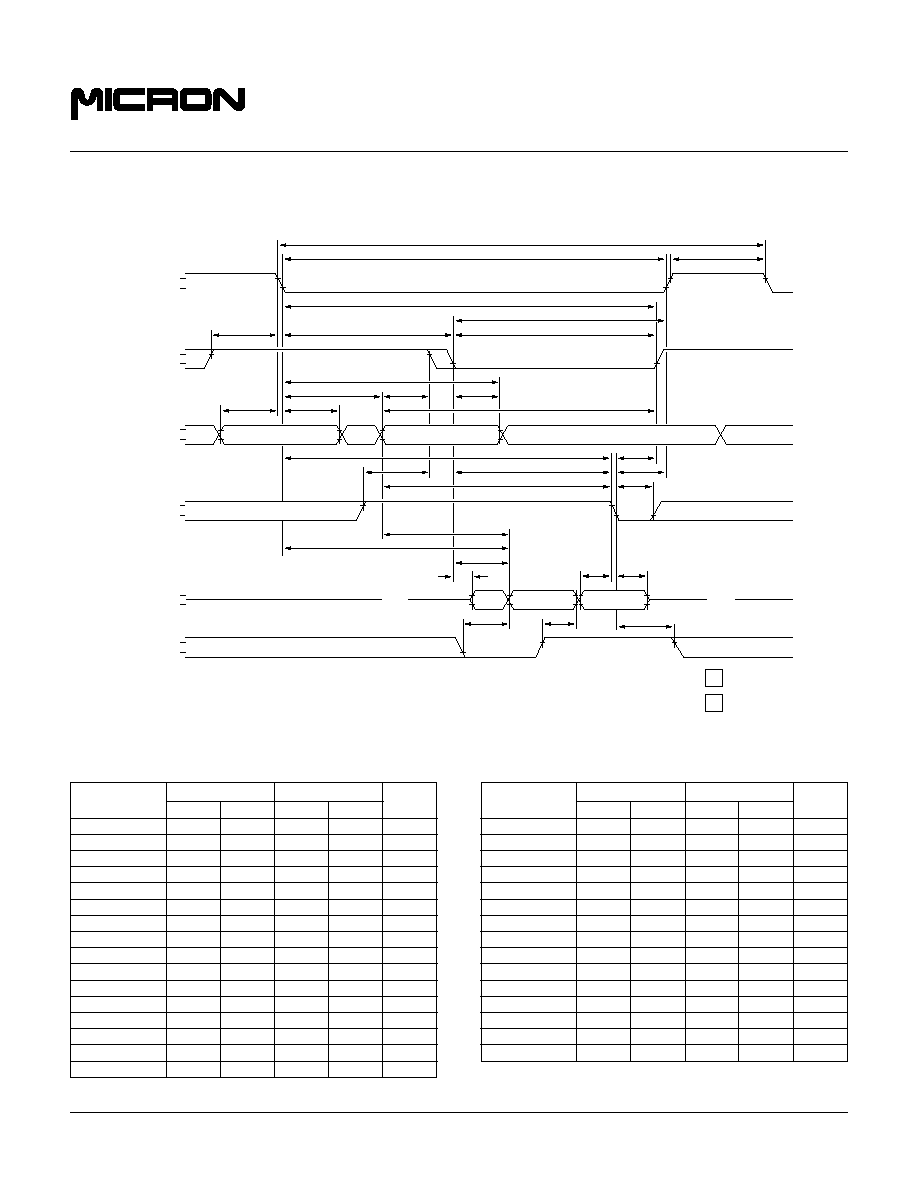
READ CYCLE
,,
,
,,
,,
,,,
,,
,
,
tRRH
,
,,,
,,
tCLZ
tCAC
tRAC
tAA
VALID DATA
OPEN
tOFF
tRCH
ROW
tRCS
tASC
tRAH
tRAD
tAR
tCAH
tRCD
tCAS
tRSH
tCSH
tRP
tRC
tRAS
tCRP
tASR
ROW
OPEN
RAS#
V
V
IH
IL
V
V
IH
IL
ADDR
V
V
IH
IL
DQ
V
V
OH
OL
V
V
IH
IL
,,,
,,,,
,,,
,,
t OD
t OE
OE#
V
V
IH
IL
COLUMN
,,,
,,,,
,,
CAS#
WE#
,,
,,,
,,,
NOTE 1
tACH
DON'T CARE
UNDEFINED
,
,
,
NOTE: 1.
t
OFF is referenced from rising edge of RAS# or CAS#, whichever occurs last.
-5
-6
SYMBOL
MIN
MAX
MIN
MAX
UNITS
t
OFF
0
12
0
15
ns
t
RAC
50
60
ns
t
RAD
9
12
ns
t
RAH
9
10
ns
t
RAS
50
10,000
60
10,000
ns
t
RC
84
104
ns
t
RCD
11
14
ns
t
RCH
0
0
ns
t
RCS
0
0
ns
t
RP
30
40
ns
t
RRH
0
0
ns
t
RSH
13
15
ns
TIMING PARAMETERS
-5
-6
SYMBOL
MIN
MAX
MIN
MAX
UNITS
t
AA
25
30
ns
t
ACH
12
15
ns
t
AR
38
45
ns
t
ASC
0
0
ns
t
ASR
0
0
ns
t
CAC
13
15
ns
t
CAH
8
10
ns
t
CAS
8
10,000
10
10,000
ns
t
CLZ
0
0
ns
t
CRP
5
5
ns
t
CSH
38
45
ns
t
OD
0
12
0
15
ns
t
OE
12
15
ns

4 Meg x 4 EDO DRAM
Micron Technology, Inc., reserves the right to change products or specifications without notice.
D47.pm5 ≠ Rev. 3/97
©
1997, Micron Technology, Inc.
12
4 MEG x 4
EDO DRAM
TECHNOLOGY, INC.
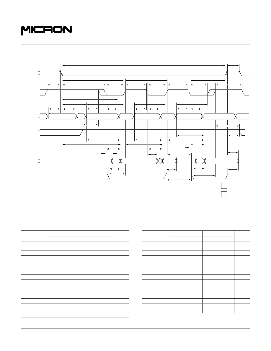
EARLY WRITE CYCLE
DON'T CARE
UNDEFINED
,
,,
,,,
,,,
,,,
,,,
,,
,,
V
V
IH
IL
,,
,
,
,,,
,,
,,
,,,
,,,
,,
VALID DATA
ROW
COLUMN
ROW
tDS
tWP
tWCH
tWCS
tWCR
tRWL
tCWL
tCAH
tASC
tRAH
tASR
tRAD
tAR
tCAS
tRSH
tCSH
tRCD
tCRP
tRAS
tRC
tRP
V
V
IH
IL
ADDR
V
V
IH
IL
V
V
IH
IL
DQ
V
V
IOH
IOL
V
V
IH
IL
RAS#
OE#
,,
,,,
,,
,,,
,,,
,,,
,,,
,,,
,,
,,
,,,
,,,
,,,
tDH
WE#
CAS#
tACH
,,,
,,,
,,
-5
-6
SYMBOL
MIN
MAX
MIN
MAX
UNITS
t
RAH
9
10
ns
t
RAS
50
10,000
60
10,000
ns
t
RC
84
104
ns
t
RCD
11
14
ns
t
RP
30
40
ns
t
RSH
13
15
ns
t
RWL
13
15
ns
t
WCH
8
10
ns
t
WCR
38
45
ns
t
WCS
0
0
ns
t
WP
5
5
ns
TIMING PARAMETERS
-5
-6
SYMBOL
MIN
MAX
MIN
MAX
UNITS
t
ACH
12
15
ns
t
AR
38
45
ns
t
ASC
0
0
ns
t
ASR
0
0
ns
t
CAH
8
10
ns
t
CAS
8
10,000
10
10,000
ns
t
CRP
5
5
ns
t
CSH
38
45
ns
t
CWL
8
10
ns
t
DH
8
10
ns
t
DS
0
0
ns
t
RAD
9
12
ns
4 Meg x 4 EDO DRAM
Micron Technology, Inc., reserves the right to change products or specifications without notice.
D47.pm5 ≠ Rev. 3/97
©
1997, Micron Technology, Inc.
13
4 MEG x 4
EDO DRAM
TECHNOLOGY, INC.
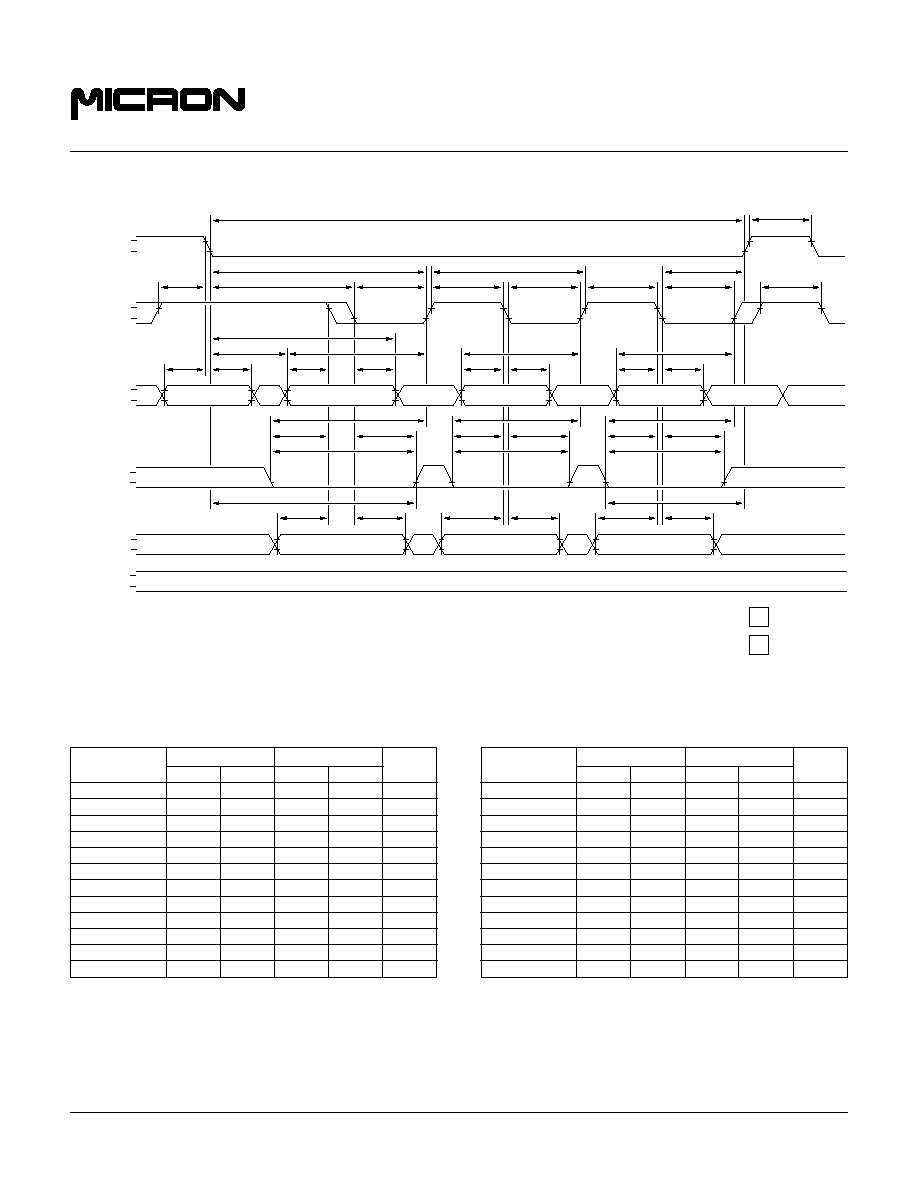
READ-WRITE CYCLE
(LATE WRITE and READ-MODIFY-WRITE cycles)
,,,
,,,
,
,
,
VALID D
OUT
VALID D
IN
,,
,,
,,
,,
ROW
,,,
,,,
,,
COLUMN
ROW
,,
,,,
,,,
,,,,
,
V
V
IH
IL
V
V
IH
IL
ADDR
V
V
IH
IL
V
V
IH
IL
DQ
V
V
IOH
IOL
V
V
IH
IL
RAS#
OPEN
OPEN
tOE
tOD
tCAC
tRAC
tAA
tCLZ
tDS
tDH
tAWD
tWP
tRWL
tCWL
tCWD
tRWD
tRCS
tASC
tCAH
tAR
tASR
tRAD
tCRP
tRCD
tCAS
tRSH
tCSH
tRAS
tRWC
tRP
tRAH
OE#
tOEH
,
,,,
,,,
WE#
tACH
CAS#
DON'T CARE
UNDEFINED
,,
,,
,
,,
,,,,
,,
-5
-6
SYMBOL
MIN
MAX
MIN
MAX
UNITS
t
OD
0
12
0
15
ns
t
OE
12
15
ns
t
OEH
8
10
ns
t
RAC
50
60
ns
t
RAD
9
12
ns
t
RAH
9
10
ns
t
RAS
50
10,000
60
10,000
ns
t
RCD
11
14
ns
t
RCS
0
0
ns
t
RP
30
40
ns
t
RSH
13
15
ns
t
RWC
116
140
ns
t
RWD
67
79
ns
t
RWL
13
15
ns
t
WP
5
5
ns
TIMING PARAMETERS
-5
-6
SYMBOL
MIN
MAX
MIN
MAX
UNITS
t
AA
25
30
ns
t
ACH
12
15
ns
t
AR
38
45
ns
t
ASC
0
0
ns
t
AWD
42
49
ns
t
ASR
0
0
ns
t
CAC
13
15
ns
t
CAH
8
10
ns
t
CAS
8
10,000
10
10,000
ns
t
CLZ
0
0
ns
t
CRP
5
5
ns
t
CSH
38
45
ns
t
CWD
28
35
ns
t
CWL
8
10
ns
t
DH
8
10
ns
t
DS
0
0
ns
4 Meg x 4 EDO DRAM
Micron Technology, Inc., reserves the right to change products or specifications without notice.
D47.pm5 ≠ Rev. 3/97
©
1997, Micron Technology, Inc.
14
4 MEG x 4
EDO DRAM
TECHNOLOGY, INC.
EDO-PAGE-MODE READ CYCLE
,
,
,,,
,,,
,,,
,,,
,,
,
,
VALID
DATA
,,
,,
VALID
DATA
,
,
VALID
DATA
,,
,
,,
,
,,
,,
,
,,
,,,
,
COLUMN
COLUMN
COLUMN
ROW
ROW
DON'T CARE
UNDEFINED
,,
,
tOD
tCAH
tASC
tCP
tRSH
tCP
tCP
tCAS
tRCD
tCRP
tPC
tCSH
tRASP
tRP
tCAH
tASC
tCAH
tASC
tAR
tRAH
tRAD
tASR
tRCS
tRRH
tRCH
tOFF
tCAC
tCPA
tAA
tCLZ
tCAC
tCPA
tAA
tCAC
tRAC
tAA
tCLZ
tOE
tOD
tOE
tOD
OPEN
OPEN
V
V
IH
IL
V
V
IH
IL
ADDR
V
V
IH
IL
V
V
IH
IL
DQ
V
V
OH
OL
V
V
IH
IL
RAS#
OE#
tCAS
tCAS
CAS#
WE#
tCOH
tOEP
tOEHC
tOES
tOES
tACH
tACH
tACH
,,
,,,,
,,
-5
-6
SYMBOL
MIN
MAX
MIN
MAX
UNITS
t
OEHC
5
10
ns
t
OEP
5
5
ns
t
OES
4
5
ns
t
OFF
0
12
0
15
ns
t
PC
20
25
ns
t
RAC
50
60
ns
t
RAD
9
12
ns
t
RAH
9
10
ns
t
RASP
50
125,000
60
125,000
ns
t
RCD
11
14
ns
t
RCH
0
0
ns
t
RCS
0
0
ns
t
RP
30
40
ns
t
RRH
0
0
ns
t
RSH
13
15
ns
TIMING PARAMETERS
-5
-6
SYMBOL
MIN
MAX
MIN
MAX
UNITS
t
AA
25
30
ns
t
ACH
12
15
ns
t
AR
38
45
ns
t
ASC
0
0
ns
t
ASR
0
0
ns
t
CAC
13
15
ns
t
CAH
8
10
ns
t
CAS
8
10,000
10
10,000
ns
t
CLZ
0
0
ns
t
COH
3
3
ns
t
CP
8
10
ns
t
CPA
28
35
ns
t
CRP
5
5
ns
t
CSH
38
45
ns
t
OD
0
12
0
15
ns
t
OE
12
15
ns
4 Meg x 4 EDO DRAM
Micron Technology, Inc., reserves the right to change products or specifications without notice.
D47.pm5 ≠ Rev. 3/97
©
1997, Micron Technology, Inc.
15
4 MEG x 4
EDO DRAM
TECHNOLOGY, INC.
EDO-PAGE-MODE EARLY WRITE CYCLE
,,
,,,
,
,,
,,
,,
,,
,,
,
,,
,,
,
,
,,
,
,,
,
,,,
,,
,,
,
,
,,
,,,
,,,
,
tDS
tDH
tDS
tDH
tDS
tDH
tWCR
VALID DATA
VALID DATA
VALID DATA
tRWL
tWP
tCWL
tWCH
tWCS
tWP
tCWL
tWCH
tWCS
tWP
tCWL
tWCH
tWCS
tCAH
tASC
tCAH
tASC
tCAH
tASC
tRAH
tASR
tRAD
tACH
tACH
tACH
tAR
COLUMN
COLUMN
COLUMN
ROW
ROW
tCP
tCAS
tRSH
tCP
tCAS
tCP
tCAS
tRCD
tCRP
tPC
tCSH
tRASP
tRP
V
V
IH
IL
CAS#
V
V
IH
IL
ADDR
V
V
IH
IL
WE#
V
V
IH
IL
DQ
V
V
IOH
IOL
RAS#
OE#
V
V
IH
IL
,,,
,,,
,,,
,,,,
,,,,
,,,
,,,
,,
DON'T CARE
UNDEFINED
,
,
,
,
,
,,,
,,
-5
-6
SYMBOL
MIN
MAX
MIN
MAX
UNITS
t
PC
20
25
ns
t
RAD
9
12
ns
t
RAH
9
10
ns
t
RASP
50
125,000
60
125,000
ns
t
RCD
11
14
ns
t
RP
30
40
ns
t
RSH
13
15
ns
t
RWL
13
15
ns
t
WCH
8
10
ns
t
WCR
38
45
ns
t
WCS
0
0
ns
t
WP
5
5
ns
TIMING PARAMETERS
-5
-6
SYMBOL
MIN
MAX
MIN
MAX
UNITS
t
ACH
12
15
ns
t
AR
38
45
ns
t
ASC
0
0
ns
t
ASR
0
0
ns
t
CAH
8
10
ns
t
CAS
8
10,000
10
10,000
ns
t
CP
8
10
ns
t
CRP
5
5
ns
t
CSH
38
45
ns
t
CWL
8
10
ns
t
DH
8
10
ns
t
DS
0
0
ns

4 Meg x 4 EDO DRAM
Micron Technology, Inc., reserves the right to change products or specifications without notice.
D47.pm5 ≠ Rev. 3/97
©
1997, Micron Technology, Inc.
16
4 MEG x 4
EDO DRAM
TECHNOLOGY, INC.
EDO-PAGE-MODE READ-WRITE CYCLE
(LATE WRITE and READ-MODIFY-WRITE cycles)
,,
,,,
,,,,
,
,,
,,
,,
,,
,
,
,
,
,,
,,
,,
,,
,,
,,,
,
DON'T CARE
UNDEFINED
,,
,,
,
,,
,,
tOE
tOE
tOE
OPEN
D OUT
VALID
DIN
VALID
D OUT
VALID
D IN
VALID
D OUT
VALID
D IN
VALID
OPEN
tDH
tDS
tAA
tCPA
tCLZ
tCAC
tDH
tDS
tAA
tCPA
tCLZ
tCAC
tDH
tDS
tAA
tCLZ
tCAC
tRAC
tWP
tCWL
tRWL
tCWD
tAWD
tWP
tCWL
tCWD
tAWD
tWP
tCWL
tCWD
tAWD
tRCS
tRWD
tASR
tRAH
tASC
tRAD
tAR
tCAH
tASC
tCAH
tASC
tCAH
tCP
tCAS
tRSH
tCP
tRP
tRASP
tCAS
tCP
tCAS
tRCD
tCSH
tPC
tCRP
ROW
COLUMN
COLUMN
COLUMN
ROW
V
V
IH
IL
CAS#
V
V
IH
IL
ADDR
V
V
IH
IL
V
V
IH
IL
DQ
V
V
IOH
IOL
V
V
IH
IL
RAS#
OE#
WE#
tPRWC
,
,,,
tOEH
tOD
tOD
tOD
NOTE 1
,,
,,,
,
NOTE: 1.
t
PC is for LATE WRITE cycles only.
-5
-6
SYMBOL
MIN
MAX
MIN
MAX
UNITS
t
OD
0
12
0
15
ns
t
OE
12
15
ns
t
OEH
8
10
ns
t
PC
20
25
ns
t
PRWC
47
56
ns
t
RAC
50
60
ns
t
RAD
9
12
ns
t
RAH
9
10
ns
t
RASP
50
125,000
60
125,000
ns
t
RCD
11
14
ns
t
RCS
0
0
ns
t
RP
30
40
ns
t
RSH
13
15
ns
t
RWD
67
79
ns
t
RWL
13
15
ns
t
WP
5
5
ns
TIMING PARAMETERS
-5
-6
SYMBOL
MIN
MAX
MIN
MAX
UNITS
t
AA
25
30
ns
t
AR
38
45
ns
t
ASC
0
0
ns
t
ASR
0
0
ns
t
AWD
42
49
ns
t
CAC
13
15
ns
t
CAH
8
10
ns
t
CAS
8
10,000
10
10,000
ns
t
CLZ
0
0
ns
t
CP
8
10
ns
t
CPA
28
35
ns
t
CRP
5
5
ns
t
CSH
38
45
ns
t
CWD
28
35
ns
t
CWL
8
10
ns
t
DH
8
10
ns
t
DS
0
0
ns

4 Meg x 4 EDO DRAM
Micron Technology, Inc., reserves the right to change products or specifications without notice.
D47.pm5 ≠ Rev. 3/97
©
1997, Micron Technology, Inc.
17
4 MEG x 4
EDO DRAM
TECHNOLOGY, INC.
EDO-PAGE-MODE READ EARLY WRITE CYCLE
(Pseudo READ-MODIFY-WRITE)
V
V
IH
IL
V
V
IH
IL
RAS#
V
V
IH
IL
ADDR
V
V
IH
IL
WE#
,,
t RASP
t RP
ROW
,,
COLUMN (A)
,,
,
COLUMN (N)
,,
,,
ROW
V
V
IH
IL
OE#
V
V
IOH
IOL
tCRP
t CSH
t CAS
t RCD
tASR
t RAH
tRAD
t ASC
tAR
t CAH
t ASC
t CAH
t ASC
t CAH
t CP
t RSH
VALID DATA
IN
,,,
,,,,
,,
,
,,
,
t RCS
t RCH
t WCS
tOE
VALID
DATA (B)
VALID DATA (A)
t WHZ
tCAC
tCPA
tAA
tCAC
tAA
OPEN
DQ
tPC
RAC
t
tCOH
t WCH
t DS
t DH
tPC
COLUMN (B)
t ACH
CAS#
t CAS
t CAS
t CP
t CP
DON'T CARE
UNDEFINED
,,
,
,,
,,,
,
-5
-6
SYMBOL
MIN
MAX
MIN
MAX
UNITS
t
OE
12
15
ns
t
PC
20
25
ns
t
RAC
50
60
ns
t
RAD
9
12
ns
t
RAH
9
10
ns
t
RASP
50
125,000
60
125,000
ns
t
RCD
11
14
ns
t
RCH
0
0
ns
t
RCS
0
0
ns
t
RP
30
40
ns
t
RSH
13
15
ns
t
WCH
8
10
ns
t
WCS
0
0
ns
t
WHZ
0
12
0
15
ns
TIMING PARAMETERS
-5
-6
SYMBOL
MIN
MAX
MIN
MAX
UNITS
t
AA
25
30
ns
t
ACH
12
15
ns
t
AR
38
45
ns
t
ASC
0
0
ns
t
ASR
0
0
ns
t
CAC
13
15
ns
t
CAH
8
10
ns
t
CAS
8
10,000
10
10,000
ns
t
COH
3
3
ns
t
CP
8
10
ns
t
CPA
28
35
ns
t
CRP
5
5
ns
t
CSH
38
45
ns
t
DH
8
10
ns
t
DS
0
0
ns
4 Meg x 4 EDO DRAM
Micron Technology, Inc., reserves the right to change products or specifications without notice.
D47.pm5 ≠ Rev. 3/97
©
1997, Micron Technology, Inc.
18
4 MEG x 4
EDO DRAM
TECHNOLOGY, INC.
READ CYCLE
(With WE#-controlled disable)
,,
,
,,
,
,
,
,,,
,,
tCLZ
tCAC
tRAC
tAA
VALID DATA
OPEN
tRCH
tRCS
tASC
tRAH
tRAD
tAR
tCAH
tRCD
tCAS
tCSH
tCRP
tASR
ROW
OPEN
RAS#
V
V
IH
IL
V
V
IH
IL
ADDR
V
V
IH
IL
DQ
V
V
OH
OL
V
V
IH
IL
,,,
,,,,
,,,
,,
t OD
t OE
OE#
V
V
IH
IL
COLUMN
,,,
,,,,
,
WE#
tWHZ
tWPZ
tCP
tASC
tRCS
COLUMN
,
tCLZ
DON'T CARE
UNDEFINED
,,
,
CAS#
,,
,,,
,,,
-5
-6
SYMBOL
MIN
MAX
MIN
MAX
UNITS
TIMING PARAMETERS
-5
-6
SYMBOL
MIN
MAX
MIN
MAX
UNITS
t
AA
25
30
ns
t
AR
38
45
ns
t
ASC
0
0
ns
t
ASR
0
0
ns
t
CAC
13
15
ns
t
CAH
8
10
ns
t
CAS
8
10,000
10
10,000
ns
t
CLZ
0
0
ns
t
CP
8
10
ns
t
CRP
5
5
ns
t
CSH
38
45
ns
t
OD
0
12
0
15
ns
t
OE
12
15
ns
t
RAC
50
60
ns
t
RAD
9
12
ns
t
RAH
9
10
ns
t
RCD
11
14
ns
t
RCH
0
0
ns
t
RCS
0
0
ns
t
WHZ
0
12
0
15
ns
t
WPZ
10
10
ns
4 Meg x 4 EDO DRAM
Micron Technology, Inc., reserves the right to change products or specifications without notice.
D47.pm5 ≠ Rev. 3/97
©
1997, Micron Technology, Inc.
19
4 MEG x 4
EDO DRAM
TECHNOLOGY, INC.
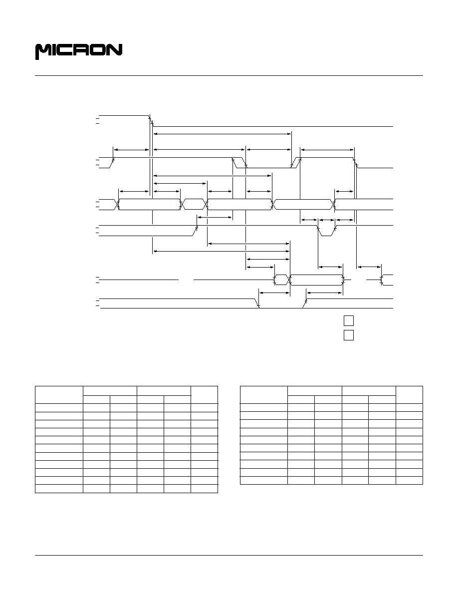
RAS#-ONLY REFRESH CYCLE
(OE# and WE# = DON'T CARE)
,,,
,,,
,,,,
,
,,
ROW
V
V
IH
IL
CAS#
V
V
IH
IL
ADDR
V
V
IH
IL
RAS#
tRC
tRAS
tRP
tCRP
tASR
tRAH
ROW
OPEN
DQ
V
V
OH
OL
tRPC
CBR REFRESH CYCLE
(Addresses and OE# = DON'T CARE)
tRP
V
V
IH
IL
RAS#
tRAS
OPEN
tCHR
tCSR
V
V
IH
IL
V
V
OH
OL
CAS#
DQ
tRP
tRAS
tRPC
tCSR
tRPC
tCHR
tCP
V
V
IH
IL
tWRP
tWRH
,
,,,
,,,
,
,,,
,,
,,
,,,
,,
WE#
tWRP
tWRH
DON'T CARE
UNDEFINED
,,
,,
,
-5
-6
SYMBOL
MIN
MAX
MIN
MAX
UNITS
t
RAS
50
10,000
60
10,000
ns
t
RC
84
104
ns
t
RP
30
40
ns
t
RPC
5
5
ns
t
WRH
8
10
ns
t
WRP
8
10
ns
TIMING PARAMETERS
-5
-6
SYMBOL
MIN
MAX
MIN
MAX
UNITS
t
ASR
0
0
ns
t
CHR
8
10
ns
t
CP
8
10
ns
t
CRP
5
5
ns
t
CSR
5
5
ns
t
RAH
9
10
ns
4 Meg x 4 EDO DRAM
Micron Technology, Inc., reserves the right to change products or specifications without notice.
D47.pm5 ≠ Rev. 3/97
©
1997, Micron Technology, Inc.
20
4 MEG x 4
EDO DRAM
TECHNOLOGY, INC.
HIDDEN REFRESH CYCLE
24
(WE# = HIGH; OE# = LOW)
,
,
DON'T CARE
UNDEFINED
,,
,
tCLZ
tOFF
,
,,,
,,,
,,,
,,,
,,
,,
,,
,
,
OPEN
VALID DATA
OPEN
COLUMN
ROW
tCAC
tRAC
tAA
tCAH
tASC
tRAH
tASR
tRAD
tAR
tCRP
tRCD
tRSH
tRAS
tRP
tCHR
tRAS
DQ
V
V
OH
OL
V
V
IH
IL
ADDR
V
V
IH
IL
V
V
IH
IL
RAS#
,
,,,
,,,,
,,,
V
V
IH
IL
tOE
tOD
OE#
tORD
,
,,,
,,
CAS#
-5
-6
SYMBOL
MIN
MAX
MIN
MAX
UNITS
t
OE
12
15
ns
t
OFF
0
12
0
15
ns
t
ORD
0
0
ns
t
RAC
50
60
ns
t
RAD
9
12
ns
t
RAH
9
10
ns
t
RAS
50
10,000
60
10,000
ns
t
RCD
11
14
ns
t
RP
30
40
ns
t
RSH
13
15
ns
TIMING PARAMETERS
-5
-6
SYMBOL
MIN
MAX
MIN
MAX
UNITS
t
AA
25
30
ns
t
AR
38
45
ns
t
ASC
0
0
ns
t
ASR
0
0
ns
t
CAC
13
15
ns
t
CAH
8
10
ns
t
CHR
8
10
ns
t
CLZ
0
0
ns
t
CRP
5
5
ns
t
OD
0
12
0
15
ns
4 Meg x 4 EDO DRAM
Micron Technology, Inc., reserves the right to change products or specifications without notice.
D47.pm5 ≠ Rev. 3/97
©
1997, Micron Technology, Inc.
21
4 MEG x 4
EDO DRAM
TECHNOLOGY, INC.
SELF REFRESH CYCLE
(Addresses and OE# = DON'T CARE)
V
V
IH
IL
RAS#
tRASS
OPEN
V
V
IH
IL
V
V
OH
OL
DQ
tRPC
tCHD
tRPS
tRPC
tRP
tCP
CAS#
,
,,,
,,
WE#
V
V
IH
IL
tWRH
tWRP
,,
,,
,,,
,,,,
,,,,
,,
tWRH
tWRP
(
)
(
)
(
)
(
)
(
)
(
)
(
)
(
)
(
)
(
)
(
)
(
)
NOTE 1
tCSR
,,
,,,,
,,,
,,,
,,,
,
,,
,,
DON'T CARE
UNDEFINED
tCP
NOTE 2
(
)
(
)
(
)
(
)
NOTE: 1. Once
t
RASS (MIN) is met and RAS# remains LOW, the DRAM will enter Self Refresh mode.
2. Once
t
RPS is satisfied, a complete burst of all rows should be executed.
-5
-6
SYMBOL
MIN
MAX
MIN
MAX
UNITS
t
RPC
5
5
ns
t
RPS
90
105
ns
t
WRH
8
10
ns
t
WRP
8
10
ns
TIMING PARAMETERS
-5
-6
SYMBOL
MIN
MAX
MIN
MAX
UNITS
t
CHD
15
15
ns
t
CP
8
10
ns
t
CSR
5
5
ns
t
RASS
100
100
µ
s
t
RP
30
40
ns
4 Meg x 4 EDO DRAM
Micron Technology, Inc., reserves the right to change products or specifications without notice.
D47.pm5 ≠ Rev. 3/97
©
1997, Micron Technology, Inc.
22
4 MEG x 4
EDO DRAM
TECHNOLOGY, INC.
24/26-PIN PLASTIC SOJ (300 mil)
DA-2
R
.299 (7.59)
.305 (7.75)
.679 (17.25)
.673 (17.09)
.340 (8.64)
.330 (8.38)
.050 (1.27) TYP
.600 (15.24) TYP
PIN #1 INDEX
.020 (0.51)
.015 (0.38)
.132 (3.35)
.142 (3.61)
.109 (2.77)
.094 (2.39)
.260 (6.60)
.275 (6.99)
.030 (0.76)
.040 (1.02)
SEATING PLANE
.025 (0.64)
MIN
.037 (0.94) MAX
DAMBAR PROTRUSION
.026 (0.66)
.032 (0.81)
NOTE:
1. All dimensions in inches (millimeters)
MAX
or typical where noted.
MIN
2. Package width and length do not include mold protrusion; allowable mold protrusion is .01" per side.
4 Meg x 4 EDO DRAM
Micron Technology, Inc., reserves the right to change products or specifications without notice.
D47.pm5 ≠ Rev. 3/97
©
1997, Micron Technology, Inc.
23
4 MEG x 4
EDO DRAM
TECHNOLOGY, INC.
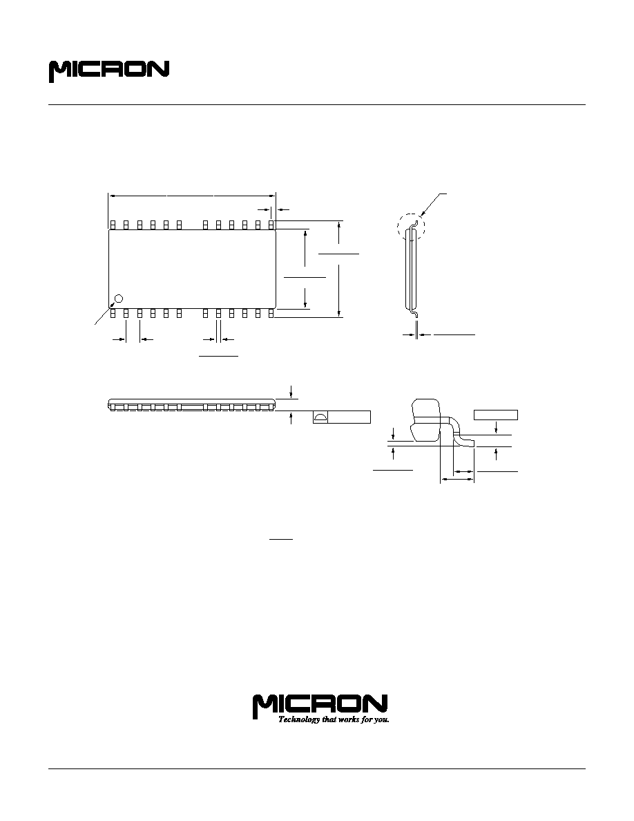
24/26-PIN PLASTIC TSOP (300 mil)
DB-2
.047 (1.20)
MAX
.367 (9.32)
.359 (9.12)
.302 (7.67)
.298 (7.57)
.050 (1.27)
TYP
.678 (17.23)
.672 (17.07)
.020 (0.50)
.012 (0.30)
PIN #1 INDEX
.037 (0.95)
SEE DETAIL A
.007 (0.18)
.005 (0.13)
.004 (0.10)
.024 (0.60)
.016 (0.40)
.006 (0.15)
.002 (0.05)
DETAIL A
.010 (0.25)
.032 (0.80)
TYP
GAGE PLANE
SEATING PLANE
NOTE:
1. All dimensions in inches (millimeters)
MAX
or typical where noted.
MIN
2. Package width and length do not include mold protrusion; allowable mold protrusion is .01" per side.
8000 S. Federal Way, P.O. Box 6, Boise, ID 83707-0006, Tel: 208-368-3900, Micron DataFax: 208-368-5800
E-mail: prodmktg@micron.com, Internet: http://www.micron.com, Customer Comment Line: 800-932-4992